
Using metamaterials, scientists have successfully designed and built the world’s first semiconductor-free, optically-controlled microelectronic device, according to a report from UPI.
The new device is 1,000% more conductive, but boasts a much smaller band gap. This means that the device’s conductivity can be triggered by a very low voltage and laser pulse.
Electrical engineering professor and researcher Dan Sievenpiper says,
This certainly won’t replace all semiconductor devices, but it may be the best approach for certain specialty applications.
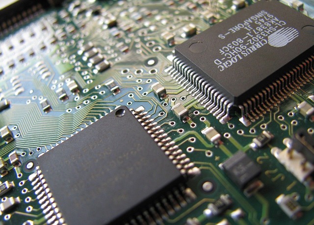
Modern technology would have never developed in the way it has without semiconductors. But like most materials, the benefits of semiconductors do come with constraints. Semiconductors put up with various levels of resistance, which constrains electron velocity. In addition, their relatively large band gaps require initial bolts of energy to trigger conductivity.
For some microelectronic components such as transistors, these pitfalls are particularly problematic.
In large electronic devices with large semiconductor components, large jolts of energy, high temperatures or strong laser pulses can lessen the impediments and get electrons flowing freely. These strategies, however, don’t work in smaller components.
Researchers at the University of California San Diego sidestepped these problems by abandoning semiconductor materials in favor of metamaterials. Metamaterials are powered by a metasurface, which are gold mushroom-like nanostructures etched onto an array of parallel gold strips. The metasurface is fixed to a silicon wafer and buffered by a layer of silicon dioxide.
When a small amount of power – less than 10 volts – and a low-power infrared laser are applied to the metasurface, the gold nanostructures generate “hot spots”. Hot spots are intense electric fields strong enough to decouple electrons from the material. The electrons are then pulled from the underlying material and allowed to move uninhibited.
The researchers described their breakthrough device in paper published in the in the journal Nature Communications.
“Next we need to understand how far these devices can be scaled and the limits of their performance,” Sievenpiper concluded.